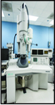
Description: The Philips CM200 ST is a versatile instrument that is designed for analysis of the physical, chemical and magnetic microstructure at high spatial resolution. EDS by EDAX, measuring x-rays emiited by the sample, GATAN imaging filter, eels electron energy loss spectrometer, energy imaging, shifted energy imaging, In addition to high resolution imaging capability, the machine is optimized for analytical electron microscopy and Lorentz imaging, under normal and applied magnetic fields. 3 cameras, scanning mode. Spatially resolved compositional analysis by X-ray emission spectroscopy (Z > 5), local electronic structure measurements by electron energy-loss spectroscopy (Z > 2), convergent beam electron diffraction for three-dimensional structure information, and energy-filtered imaging at the nanometer scale are some of the techniques available on this instrument. 2 angstrums. brightfield imaging, 1 million magnification.
POC and Phone #: Joel Alexa
757.864.8721E-mail: robert.a.edahl@nasa.gov
Location: Bldg 1205; Rm 152
Manufacturer: Philip |
 |
|